1 厦门大学公共卫生学院 传染病疫苗研发全国重点实验室 翔安创新实验室厦门 361102
2 福建汇盛生物科技有限公司漳州 363000
电子束(Electron beam,EB)辐照灭菌是避免微生物污染影响食物品质的有效方法。为探究南美白对虾使用电子束灭菌后的性能变化,采用10 MeV电子加速器辐照加工系统对样品进行辐照(吸收剂量范围0~12 kGy),并对虾的蛋白质、脂肪和氨基酸含量,pH,挥发性盐基氮,质构特征,微生物学及感官满意度进行测试。结果表明:蛋白质、脂肪含量均在正常范围内。在最佳吸收剂量(6~8 kGy)时,表征虾新鲜度的挥发性盐基氮含量较低,大部分氨基酸含量达峰值,咀嚼性、内聚性等质构特征明显提升,未检出微生物菌落,颜色和口感更好。这表明EB辐照灭菌是一种有效的食品微生物控制手段,在不降低冷冻南美白对虾营养成分等性能的情况下,使其口感更为新鲜。
南美白对虾 电子束辐照 灭菌 Litopenaeus vannamei Electron beam irradiation Sterilization 辐射研究与辐射工艺学报
2023, 41(6): 060404

Author Affiliations
Abstract
1 National University of Singapore, Department of Electrical and Computer Engineering, Singapore
2 A*STAR (Agency for Science, Technology and Research), Institute of Microelectronics, Singapore
3 Huazhong University of Science and Technology, School of Optical and Electronic Information, Wuhan National Laboratory for Optoelectronics, Wuhan, China
4 Nanyang Technological University, Quantum Science and Engineering Centre, Singapore
Lithium niobate (LN) has experienced significant developments during past decades due to its versatile properties, especially its large electro-optic (EO) coefficient. For example, bulk LN-based modulators with high speeds and a superior linearity are widely used in typical fiber-optic communication systems. However, with ever-increasing demands for signal transmission capacity, the high power and large size of bulk LN-based devices pose great challenges, especially when one of its counterparts, integrated silicon photonics, has experienced dramatic developments in recent decades. Not long ago, high-quality thin-film LN on insulator (LNOI) became commercially available, which has paved the way for integrated LN photonics and opened a hot research area of LN photonics devices. LNOI allows a large refractive index contrast, thus light can be confined within a more compact structure. Together with other properties of LN, such as nonlinear/acousto-optic/pyroelectric effects, various kinds of high-performance integrated LN devices can be demonstrated. A comprehensive summary of advances in LN photonics is provided. As LN photonics has experienced several decades of development, our review includes some of the typical bulk LN devices as well as recently developed thin film LN devices. In this way, readers may be inspired by a complete picture of the evolution of this technology. We first introduce the basic material properties of LN and several key processing technologies for fabricating photonics devices. After that, various kinds of functional devices based on different effects are summarized. Finally, we give a short summary and perspective of LN photonics. We hope this review can give readers more insight into recent advances in LN photonics and contribute to the further development of LN related research.
lithium niobate etching photonics integrated optics nanotechnology devices Advanced Photonics
2022, 4(3): 034003

Author Affiliations
Abstract
Institute of Microelectronics, A*STAR (Agency for Science, Technology and Research), Singapore 138634, Singapore
Gas sensors have a wide variety of applications. Among various existing gas sensing technologies, optical gas sensors have outstanding advantages. The development of the Internet of Things and consumer electronics has put stringent requirements on miniaturized gas sensing technology. Here, we demonstrate a chip-scale silicon substrate-integrated hollow waveguide (Si-iHWG) to serve as an optical channel and gas cell in an optical gas sensor. It is fabricated through silicon wafer etching and wafer bonding. The Si-iHWG chip is further assembled with an off-chip light source and detector to build a fully functional compact nondispersive infrared (NDIR) sensor. The chip size is , and the dimension of the sensor excluding the microcontroller board is . This chip solution with compactness, versatility, robustness, and low cost provides a cost-effective platform for miniaturized optical sensing applications ranging from air quality monitoring to consumer electronics.
Photonics Research
2022, 10(1): 01000261
Author Affiliations
Abstract
1 Institute of Microelectronics, A*STAR (Agency for Science, Technology and Research), Singapore 138634, Singapore
2 Current Address: School of Microelectronics Science and Technology, Sun Yat-sen University, Zhuhai 519082, China
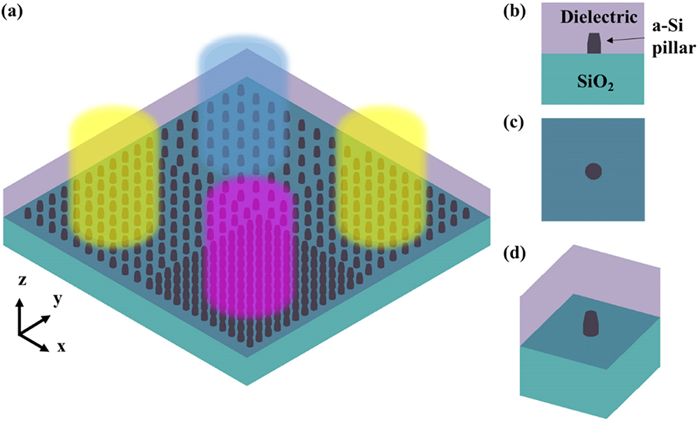
Optical color filters are widely applied in many areas including display, imaging, sensing, holography, energy harvest, and measurement. Traditional dye-based color filters have drawbacks such as environmental hazards and instability under high temperature and ultraviolet radiation. With advances in nanotechnology, structural color filters, which are based on the interaction of light with designed nanostructures, are able to overcome the drawbacks. Also, it is possible to fabricate structural color filters using standard complementary metal-oxide-semiconductor (CMOS) fabrication facilities with low cost and high volume. In this work, metasurface-based subtractive color filters (SCFs) are demonstrated on 12-inch (300-mm) glass wafers using a CMOS-compatible fabrication process. In order to make the transmissive-type SCF on a transparent glass wafer, an in-house developed layer transfer process is used to solve the glass wafer handling issue in fabrication tools. Three different heights of embedded silicon nanopillars (110, 170, and 230 nm) are found to support magnetic dipole resonances. With pillar height and pitch variation, SCFs with different displayed colors are achieved. Based on the resonance wavelength, the displayed color of the metasurface is verified within the red-yellow-blue color wheel. The simulation and measurement results are compared and discussed. The work provides an alternative design for high efficiency color filters on a CMOS-compatible platform, and paves the way towards mass-producible large-area metasurfaces.
Photonics Research
2021, 9(1): 01000013
1 华中科技大学武汉光电国家研究中心, 湖北 武汉 430074
2 重庆光电技术研究所, 重庆 南坪 400060
荧光光谱分析是一种重要的测试手段。近年来,基于光纤探针的荧光测试技术成为研究热点,这种方法具有高效、微观、实时、原位、体积小易集成等优势。简要综述荧光分析原理、光纤探针中激光发射与荧光收集的空间传导理论,以及光纤荧光探针的典型结构与制备,总结了应用于生物、环境和食品安全领域的研究状况。最后,对光纤荧光探针的发展趋势进行了展望。
激光光学 光纤探针 荧光 传导理论 探针结构 激光与光电子学进展
2020, 57(1): 010003
1 南京信息工程大学 电子与信息工程学院,江苏 南京 210044
2 南京信息工程大学 数理学院,江苏 南京 210044
3 广西师范大学 电子工程学院, 广西 桂林 541004
文章给出了一种基于光纤布拉格光栅(FBG)阵列的可调谐二维编解码器结构。重点分析了在波长不匹配时由于编解码器解码输出的自相关峰值功率削弱,进而劣化系统的误码率的情况。仿真了随着跳频扩时(TS/WH)码字参数的变化,编解码器在相应波长发生偏差条件下的解码输出功率和误码率。分析结果表明,当波长偏差0.1 nm时,对于跳频个数为31的编解码器,系统的误码率仍然<10-9,因而可以通过增加跳频波长数来降低编解码器对调谐精度的要求。
光纤布拉格光栅阵列 波长偏差 可调谐编解码器 误码率 FBG array wavelength mismatch tunable coder/decoder BER
1 南京信息工程大学数理学院, 江苏 南京 210044
2 广西师范大学电子工程学院, 广西 桂林 541004
以光子晶体缺陷模理论和慢光效应为基础,提出了一种基于光子晶体的多通道滤波器结构用于二维光码分多址(2D-OCDMA)系统编解码的方案,并分析其编码性能。根据耦合模理论,通过缺陷谐振腔的滤波作用,用户光信号按地址码序列切割成多个脉冲序列,完成对用户信号的谱域编码。由于光子晶体波导的慢光效应,微米量级编码器结构的时延可以达到纳米量级,达到正确编解码的标准。设计的2D-OCDMA三码片编码器中心波长分别为1545.00,1555.30和1570.60 nm,缺陷间隔时延为0.4 ns。由于透射谱几乎不存在旁瓣,所以解码时信号基本上不会出现干扰,保证了用户发送和接收信号的准确性。
光学器件 光子晶体 二维光码分多址编解码器 慢光效应 缺陷模 光学学报
2010, 30(s1): s100204


